CalmSmile Intelligent Technology
Fix IT immediately!
LCD Panel
LCD Connectors
Timing controller,LVDS Receiver,EDP,MIPI,TTL,Backlight connector,Source Driver,Gate Driver
LCD Parameters
LVDS Logic Input Voltage,LVDS signal definition,Display resolution (pixel),Overall dimension (mm),Screen size (inch) and more
LCD Brands
Auo,Boe,Chimei-Innolux,Chungwa,LG-Philips,Mitsubishi,Nec,Panasonic,Samsung,Sharp,Tianma etc.
LCD Specifications
outline,structure and principle,applications,general specifications,absolute maximum ratings,block diagram,mechanical specifications,electrical characteristics,driving for lcd,driving for backlight,connections and functions for interface pins,lvds,backlight,position of plugs and a socket,connection between receiver and transmitter for lvds,display colors and input datasignals,interface timing,timing characteristics,input signal timing chart,pixel data alignment of display image,power supply voltage sequence,optics,markings
-
InfoVision M156GWFA R0 15.6″ FHD LCD Panel
-
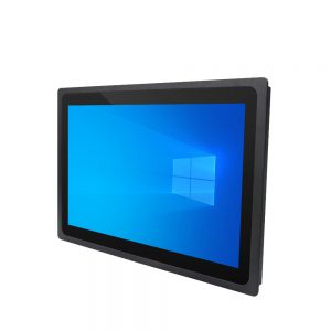
21.5 inch industrial embedded capacitive touch All in one PC
-
18.5 inch industrial embedded capacitive touch All in one PC 1920×1080
-
18.5 inch industrial embedded capacitive touch All in one PC 1366×768
-
15.6 inch industrial embedded capacitive touch All in one PC
-
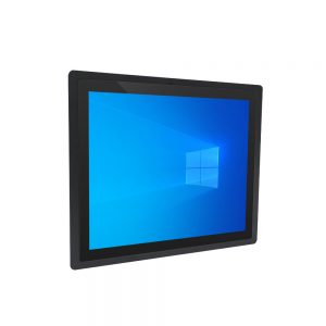
13.3 inch industrial embedded capacitive touch All in one PC
-
10.1 inch industrial embedded capacitive touch All in one PC 1920×1200
-
10.1 inch industrial embedded capacitive touch All in one PC 800×1280
-
7 inch industrial embedded capacitive touch All in one PC
-
12.1 inch industrial embedded capacitive touch All in one PC
-
10.4 inch industrial embedded capacitive touch All in one PC
-
19 inch industrial embedded capacitive touch All in one PC